This type of project allows to solve the electronic structure of an open
system formed by a finite structure sandwiched between two semi-infinite
metallic leads. A finite bias can be applied between both leads, to drive a
finite current.
The Transport workflow requires the use of the TranSIESTA 4.1 calculator
(see section The TranSIESTA calculator). TranSIESTA method calculates the non-equilibrium
density generated by the bias. To calculate the electronic structure of a
system under an external bias, the TranSIESTA code attaches the system to
semi-infinite electrodes from the left and right of the contact region.
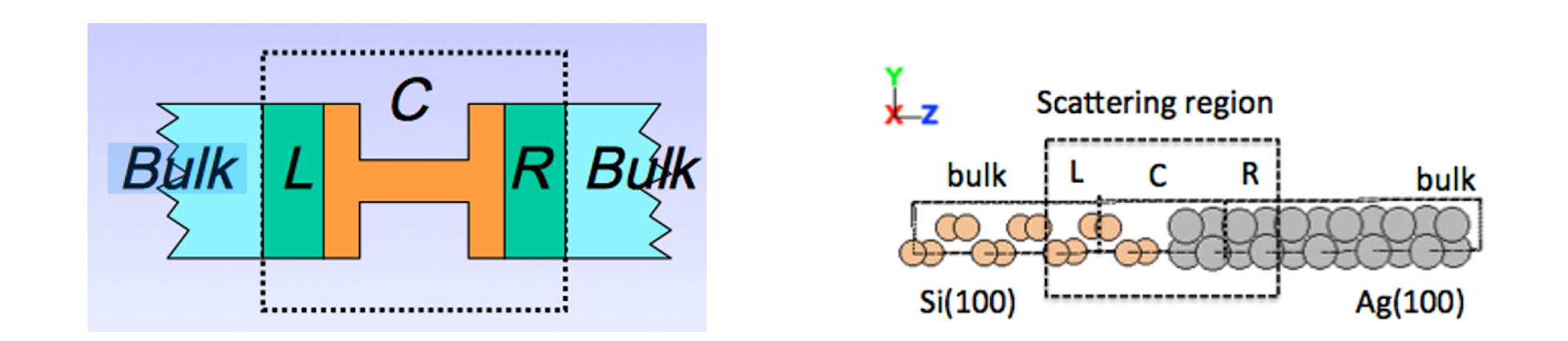
Fig. 16 Left: Schematic representation of the different parts involved in the
transport calculations. Right: example of system geometry Ag(100)/Si(100)
for transport calculation.#
Fig. 17 summarises the workflow needed to perform electronic transport
calculation and analysis,
Fig. 17 List of steps needed to compute transmission and current of an electronic
device.#
In summary, the steps are:
1. Define the atomic structure, consisting of two or three sub-systems that
must be created as separated ASAP projects,
Left and the Right bulk electrodes (Bulk): defined by two periodic
parts. Electrodes could be surfaces, nanowires, nanotubes or even atomic
chains. TranSIESTA allows to connect any amount of electrodes to a
scattering region.
Contact region or Scattering Region (SR): A finite system. It provides
the functionality of the device, and causes the charge carriers, i.e.
electrons and holes, to be scattered between two electrodes. The Scattering
Region contains the ‘contact’ (C) region, and the part of the right (R) and
left (L) electrodes. The central scattering region can be set up to include
defects, molecules or any kind of impurities.
2. Run a single point calculation of the electrode structures and contact
molecule. This step is not mandatory, but it is recommended to guarantee the
proper size for the contact region and the electrode length. (You can find
further information in sections Electrode: Single point calculation and Contact region: Single point calculation).
3. Combine the two electrodes and a contact molecule to create the target
electronic device by using the merge for transport calculation. You can
find information of the use of merge for transport calculation tool in
section Build the device: Merge electrodes and contact region.
3’. (Optional step) Compute the minimum energy (geometry optimisation) for a
set of transport device geometries. Each system is built out of two
subsystems (electrode and contact-electrode) placed at different relative
distances (d). It possibilities to start a new electronic transport project
from an optimised device geometry. You can find further information in
section Transport Device Geometry Optimisation.
4. Run the electronic transport project (automatically created after step
3). You can find further information in section Electronic transport calculations. The output of the
electronic transport project is used as input of a new project devoted to
post-process the results and compute the transmission and I-V curve of the
device.
5. Run the post-processing electronic transport project. After completion of
the project, the transport analysis widget shows the Transmission and the
Current through the device. You can find further information in section
Electronic Transport workflow: Analysis.
The left and the right electrodes can be surfaces, nanotubes or even atomic
chains. See section Structure Modeling in ASAP to learn how to use the atomic structure builder.
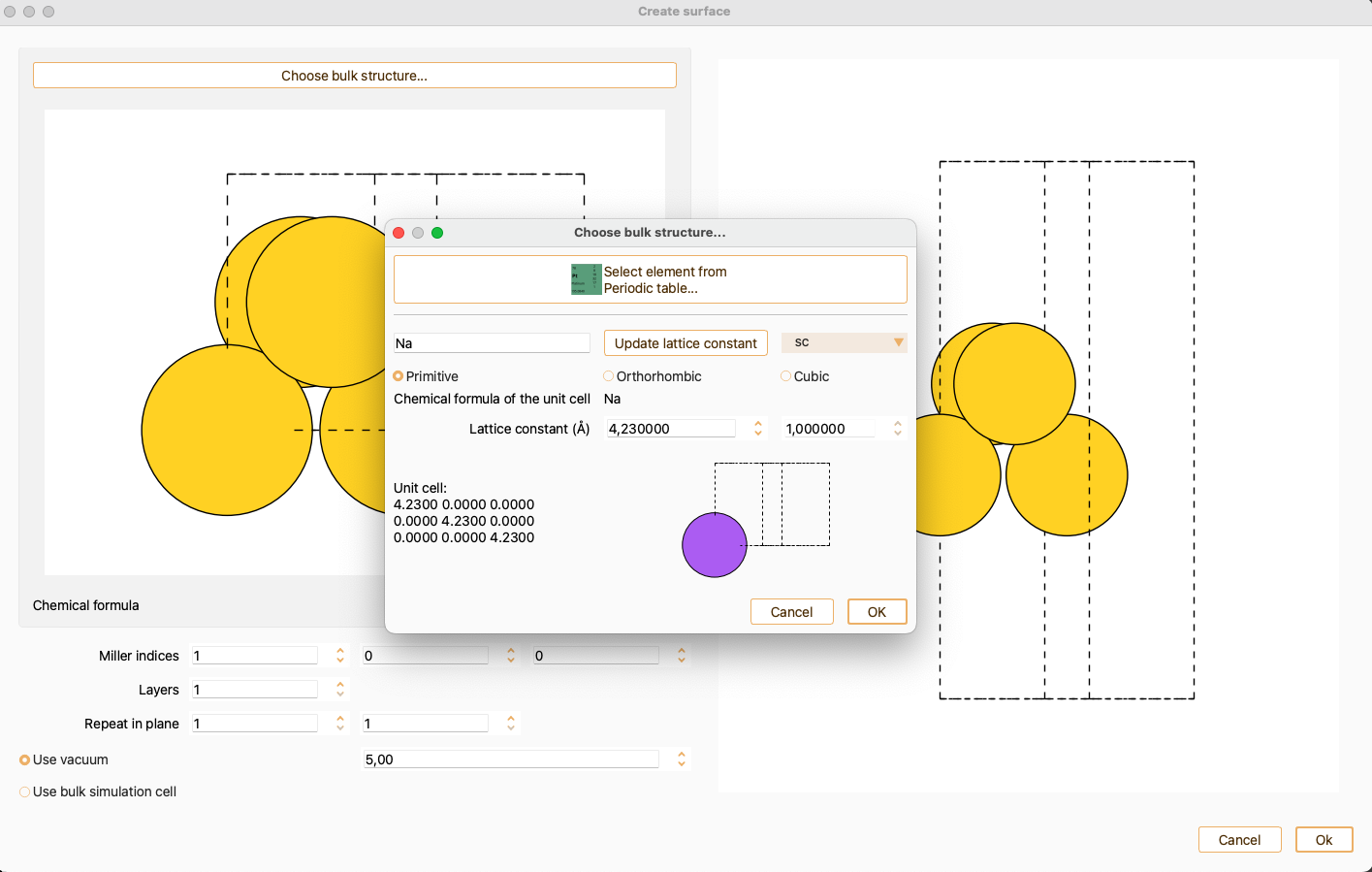
In the following example, we construct a Sodium (Na) electrode from Na bulk
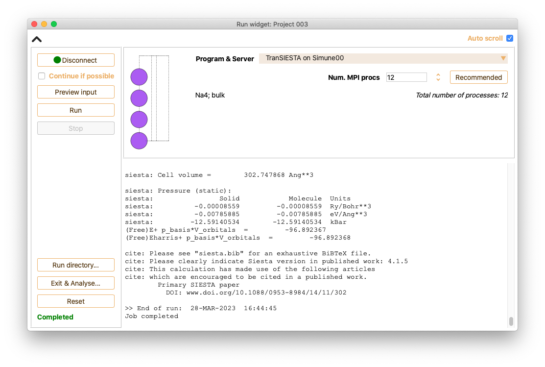
structure with simple cubic (sc) unit cell.
Notice that the Use bulk simulation cell check box is checked in the
surface builder widget. It is necessary to remove the existing vacuum along
the z direction.
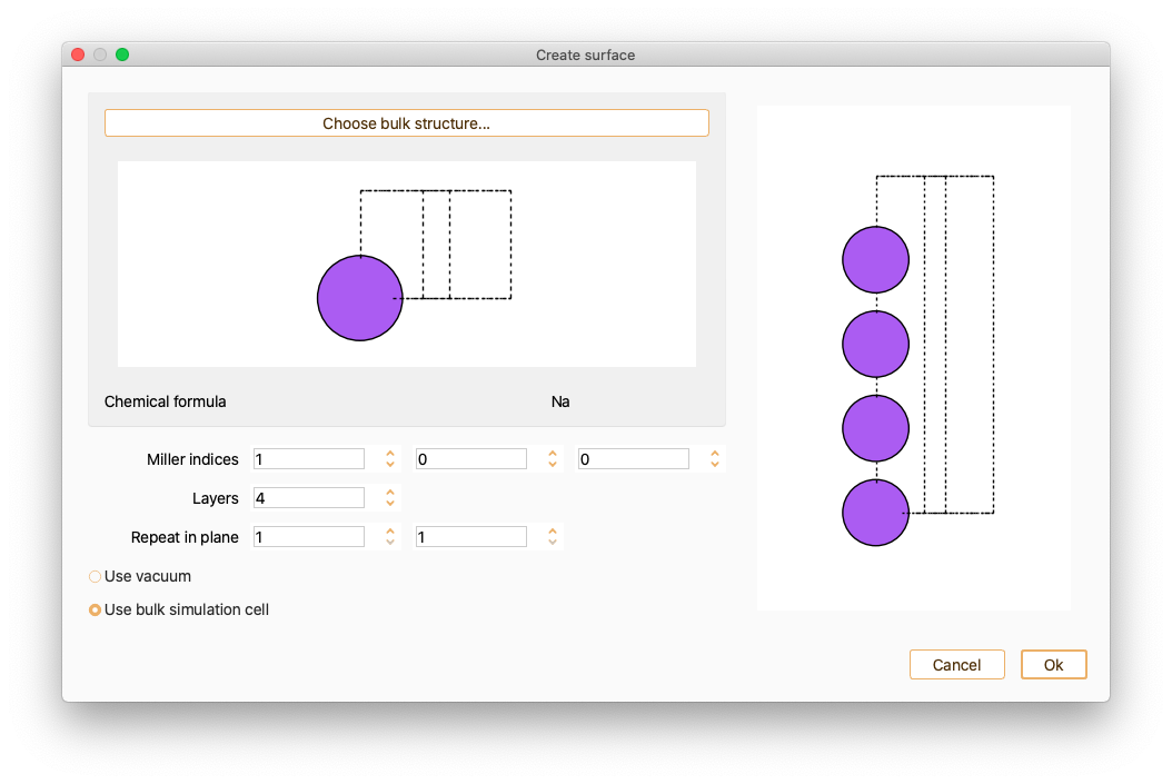
When building the electrode structure, we recommend the use of only one unit
cell for the periodic cross-section (Repeat in plane: 1, 1). The
expansion in the cross-section can be done later when using the Merge for
transport calculation tool. The expansion in the cross-section is taken
into account via Bloch expansion coefficients in TranSIESTA.
The number of Layers, 4 in the example, indicates the electrode length
along the z-axis (Transport direction).
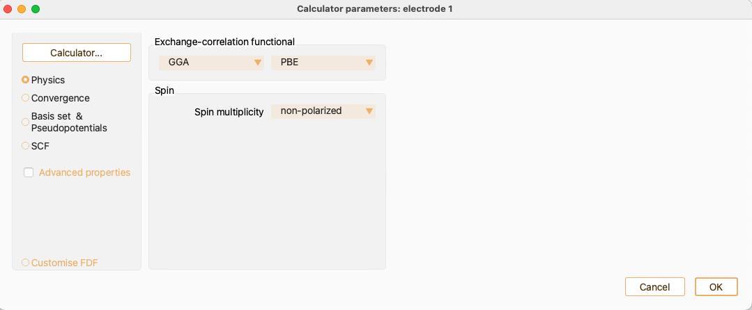
The next step after creating the electrode structure, it is to run a
Single point calculation (default project type in ASAP), selecting
TranSIESTA 4.1. as calculator.
You can tune the input variables through the calculator graphical user
interface. See section The SIESTA Calculator for further information
about the available options.
Click on the Run button,
select the Program and Server (TranSIESTA program is required), and press
Run to start the simulation.
The contact/scattering region provides the functionality of the device, and
causes the charge carriers (i.e. electrons and holes) to be scattered
between the two electrodes. The central contact region can be set up to
include defects, molecules or any kind of impurities.
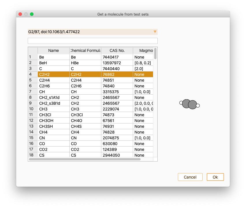
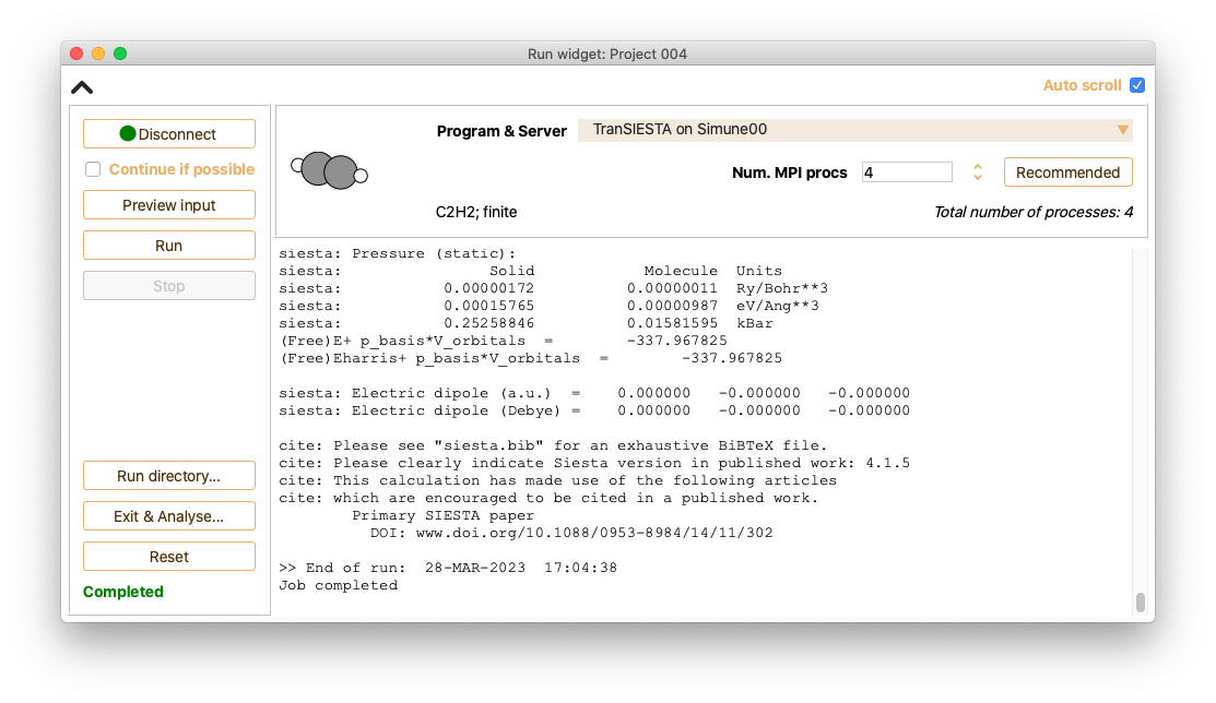
In this example, we use a ethyne molecule (C2H2) as contact in the device.
See section Structure Modeling in ASAP to learn how to create a finite structure.
The next step after creating the contact structure, it is to run a Single
point calculation (default project type in ASAP), selecting TranSIESTA 4.1.
as calculator.
Build the device: Merge electrodes and contact region#
Once the electrodes and contact region (two or three sub-systems created as
separated ASAP projects) are built, you can merge the three structures to
create the electronic device.
Completed calculations of electrodes and contact region (as the ones
described in the previous subsections, Electrode: Single point calculation and Contact region: Single point calculation) are
recommended but optional. They are used for an estimate of the minimal
electrode and contact region lengths.
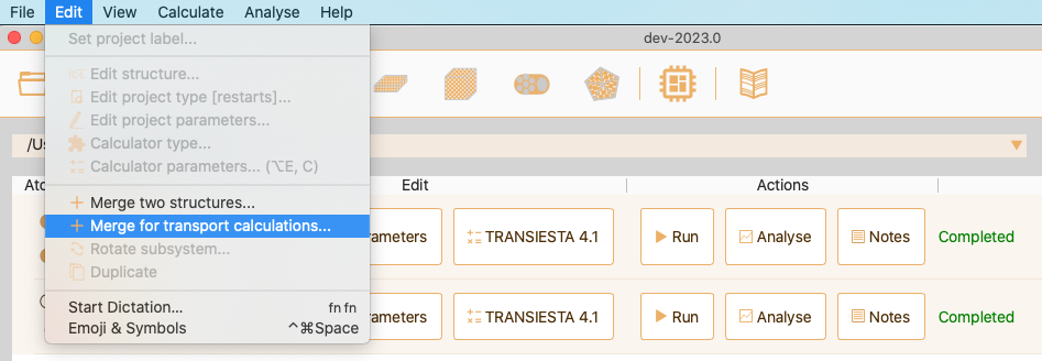
To create your electronic device, select the projects containing the
structures of electrodes and the contact region, then go to Edit and
click on the option Merge for transport calculations….
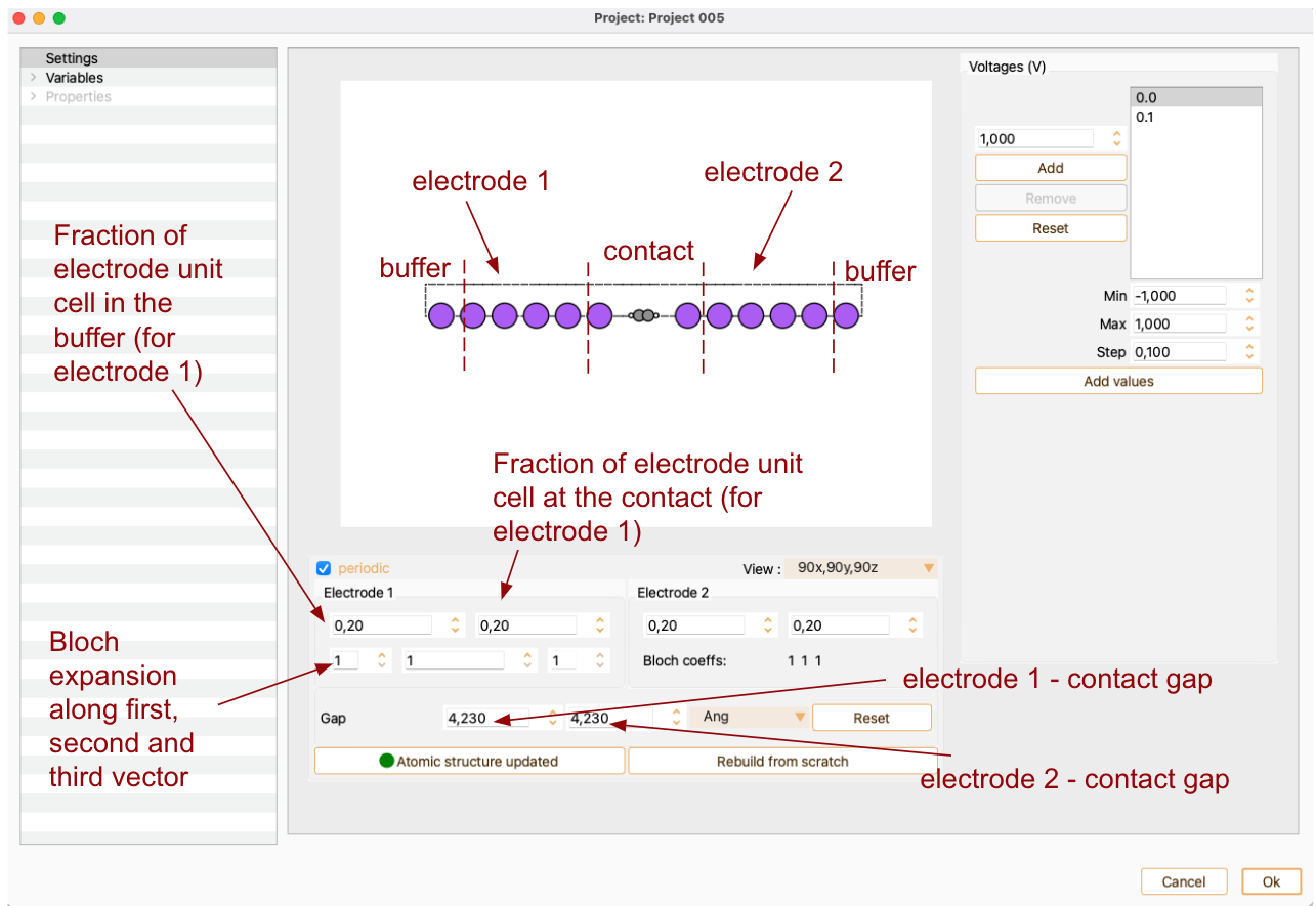
Fig. 18 shows the Merge for transport calculations widget when Na
electrodes and C2H2 contact are selected. In this example, we are considering
the two electrodes to be the same, however, three projects can be considered
in order to build a device with different left and right electrodes.
Fig. 18 Merge structure for transport calculations widget#
As it is shown in Fig. 18,
you can tailor the device structure and
size in the merge structures for transport calculation widget. You can
define the length of the contact region by tuning the Gap and the fraction
of electrode cells in the contact region.
You are referred to section Merge for transport calculations
for further information on the Merge for transport calculation tool.
The most important aspects you need to consider when building a device for
electronic transport calculations are:
The length of the electrode bulk cells and the contact region must be
sufficiently long along the transport direction. If we imagine an infinite
wire consisting of repeating electrode bulk cells, only adjacent cells must
interact. This means there should be no overlap of orbitals between
non-adjacent cells.
In the device structure, there should not be overlap of orbitals between
two bulk electrode cells.
The requirements listed above are needed for using the formalism behind
TranSIESTA calculations. If they are not fulfilled the results are
unphysical.
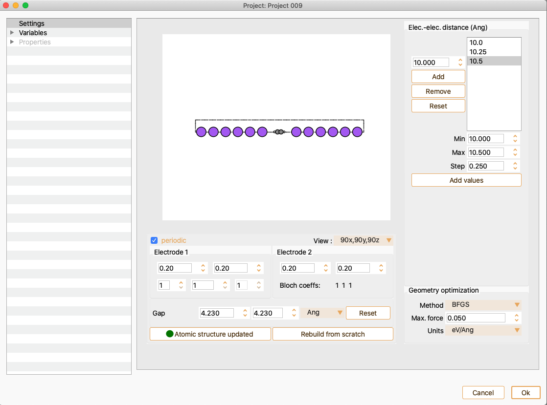
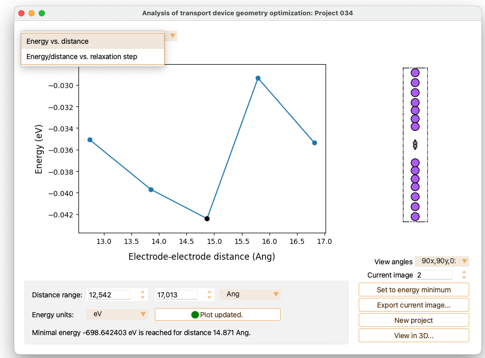
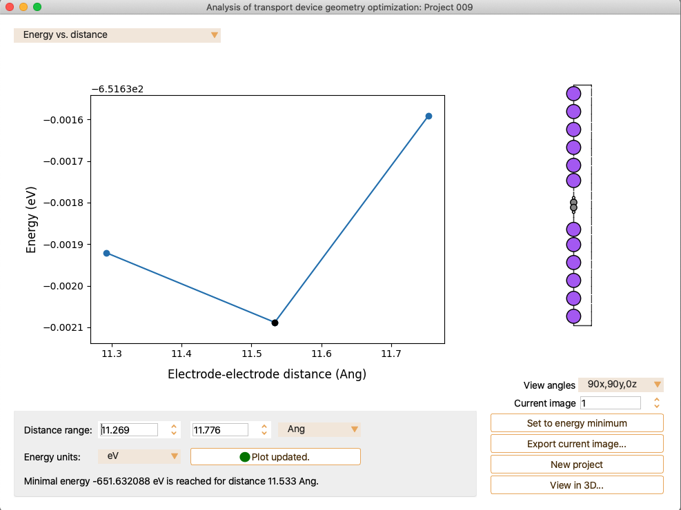
In this section, we describe the workflow for optimising the electronic
transport device geometry. In summary, we compute the minimum energy
(geometry optimisation) of a set of transport device systems. Each system is
built out of two subsystems (electrode and contact-electrode) placed at
different relative distances (d).
Optimising the electronic transport device geometry is recommended but not
mandatory. It is possible to run an electronic transport calculation, as
described in section Electronic transport calculations, without optimising the device geometry.
From the list of possible project types implemented in ASAP, select
Transport device geometry optimisation.
Then click on the Parameters icon to open the Transport Device Geometry
Optimisation parameters widget.
The Parameter widget compiles parameters that can be classified into two
categories:
Values defining the device geometry
Add: To create the list of electrode - electrode distances.
Remove: To remove the selected distance value from the list.
Reset: To sets the electrode-electrode distance to the starting
value.
ASAP offers also the possibility of automatically creating a list of
electrode - electrode distances. Use the parameters at the bottom of the
widget to introduce the minimum (Min) and maximum (Max) distance
and the interval between values (Step).
You can tune the Bloch expansion coefficients (how many times to repeat
the electrode in the cross-section) to make a wide electrode.
Input parameters for geometry optimisation
You can tuned the optimisation method (Method) and the convergence
criterion (Max. force). The force on all individual atoms should be
less than the specified maximum force.
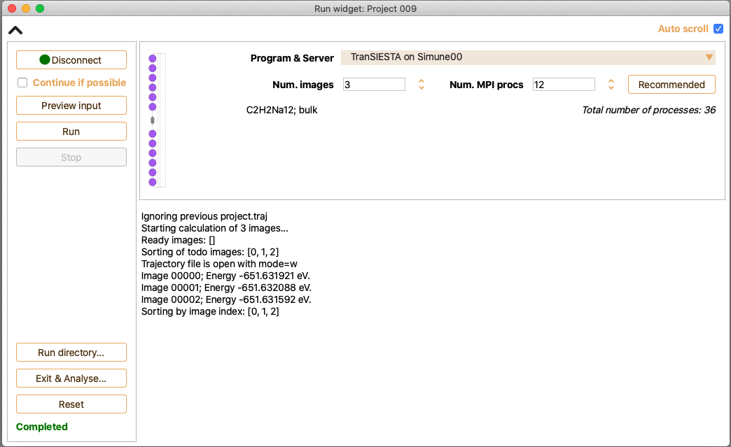
Click on the Calculator icon to select the computational engine to be used
during the device geometry optimisation. You can use either SIESTA or
TranSIESTA.
Click on the Run icon to open Run widget. Then click on the Run button
to submit the Transport Device Geometry optimisation calculation.
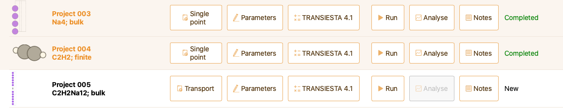
After building the device by using the Merge for transport calculation
tool, the electronic transport project is created in the project tray.
Fig. 19 Example of a created transport project from two completed projects. In the
example, electrodes right and left are equivalent. Three projects may be
considered in order to build a device with different left and right
electrodes.#
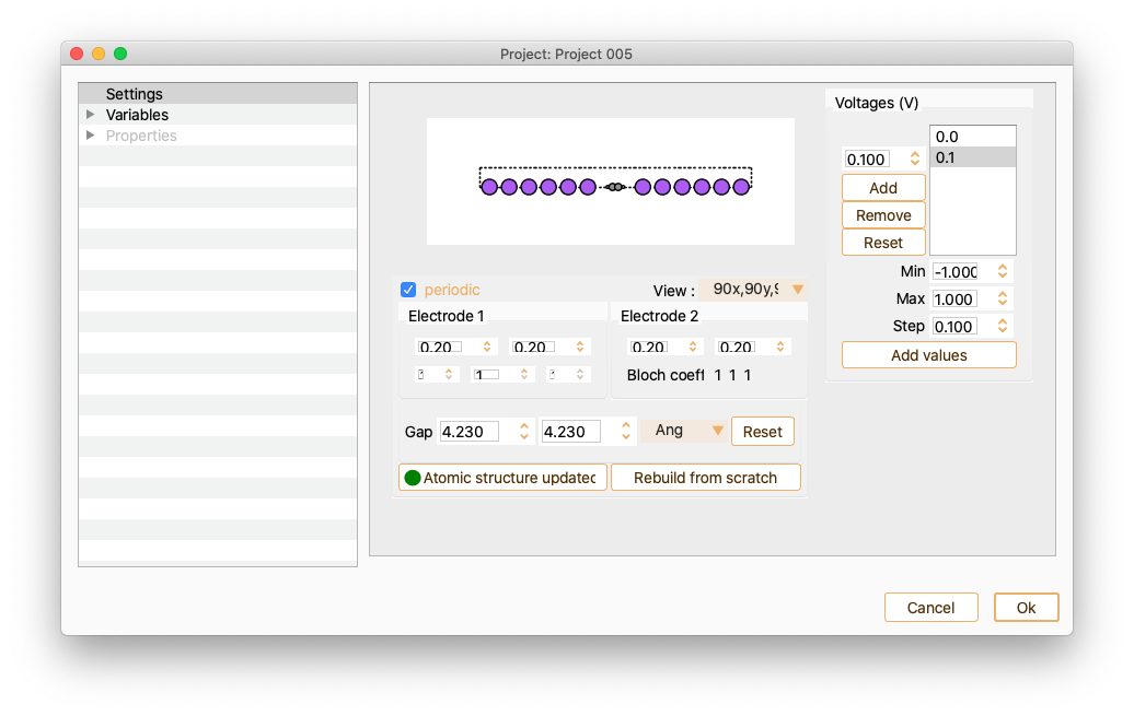
Click on the Parameters icon to open the widget to set up the input
parameters related to an electronic transport type of project.
Fig. 20 Parameter setting widget for transport calculations.#
Fig. 21 Parameter setting widget for transport calculations.#
We describe below the parameters included in the Settings tab. We refer
the user to chapter Parameters for information on other parameters (Variables)
that can be tuned.
In the right side of the widget, you can introduce a list of voltages by
using the following buttons:
Add: To add a value to the list of voltages. For each voltage, a
transport calculation will be performed. The voltage will be applied to the
system along the transport direction. The calculations are run in serial,
one after the other. It is important to increase the voltage gradually. We
suggest to use voltage steps of 0.1 V.
Remove: To remove a selected voltage value from the list on the right.
Reset: To delete the list of voltages.
It is also possible to perform an electronic transport calculation with a
voltage bias set to zero. In this case, the code will deliver the
equilibrium density of the system.
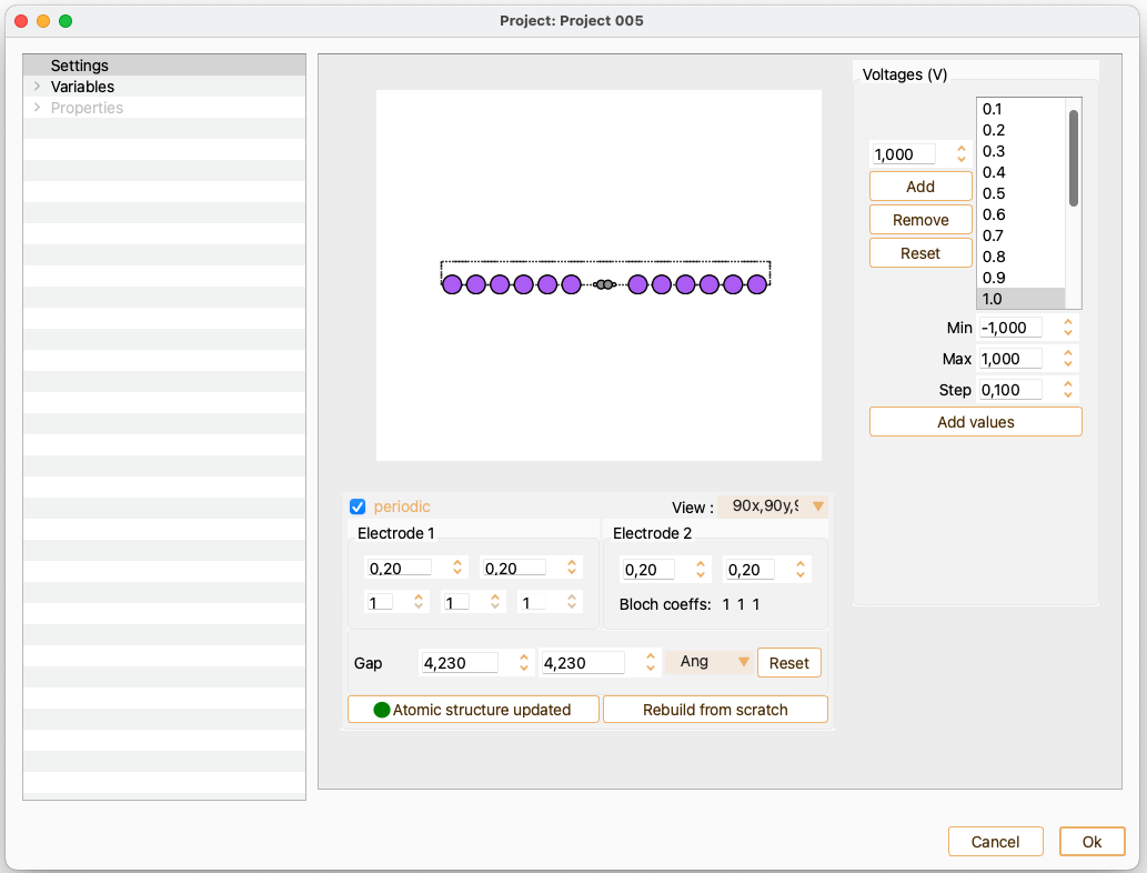
ASAP also offers the possibility of automatically creating a list of voltage
values. Press Add values to create a list of voltages from the selected
minimum (Min) and maximum (Max) values. The interval between the
values is defined by the parameter (Step). In the example shown in
Fig. 22,
the list of values is created from -1 V to 1 V by a step of 0.1 V.
Fig. 22 List of voltages created from -1 V to 1 V by a step of 0.1 V.#
Computing electronic transport with the settings shown in the Figure
Fig. 22 is computationally expensive.
In the following step, we use the
parameters shown in the Fig. 21.
In the setting tab, you can also tune the device structure and size. You can
define the length of the contact region by tuning the Gap and the fraction
of electrode cells in the contact region. Normally, it is needed to add some
electrode layers in the contact region to make electrode layers out of the
contact region behave as bulk.
Fig. 23 Parameter widget. Description of parameters to tune the device structure
and size.#
The calculator automatically associated to an electronic transport type of
project is TranSIESTA 4.1. Click on the Calculator icon if you wish to
edit the default calculator parameters.
You can read section The TranSIESTA calculator for
detailed information on TRANSIESTA input parameters.
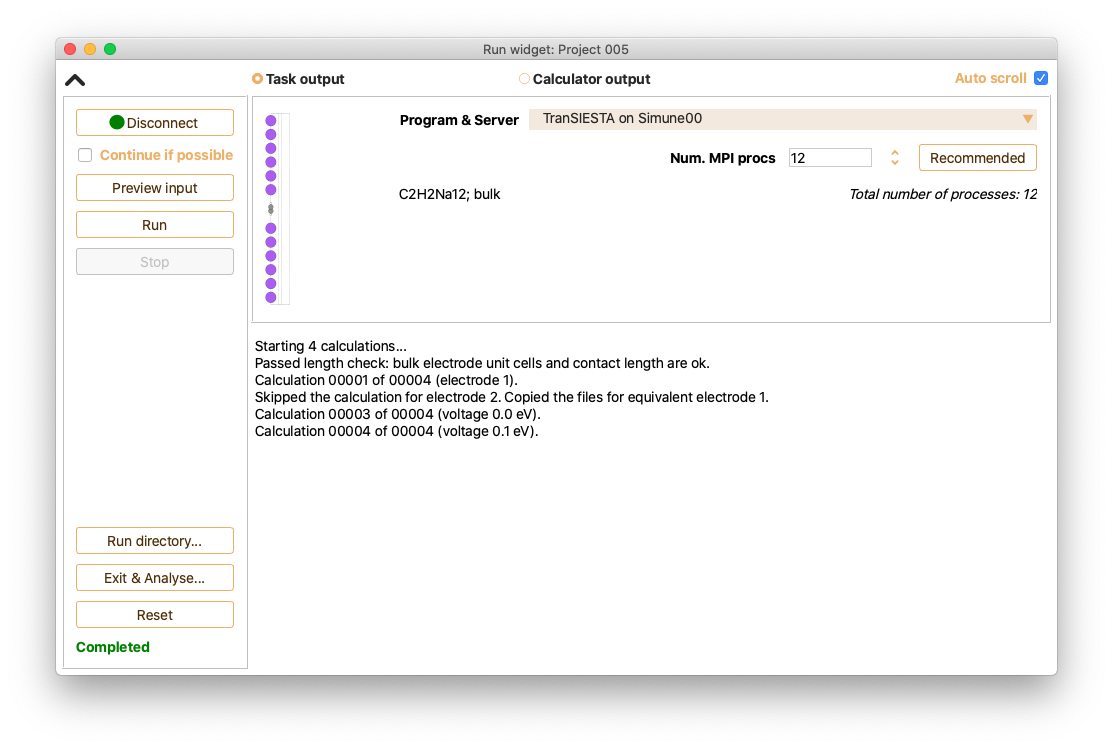
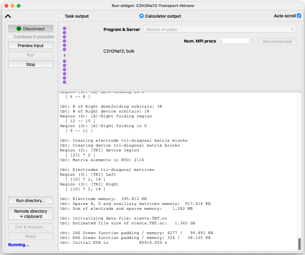
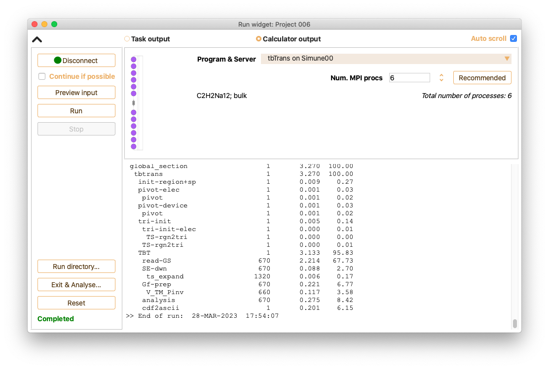
Click on the Run icon to open the Run widget.
Then click on the Run button to submit the electronic transport calculation.
You can read chapter Advanced Configuration and Remote Execution for detailed information on the computational
resources configuration in ASAP.
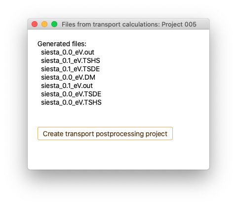
When the electronic transport calculation is completed, select Exit &
Analyse… to open the analysis widget and see the list of the generated
output files. Click on the Create transport postprocessing project
button to create a new project devoted to compute the transmission and I-V
curve of the device.
Fig. 24 New transport postprocessing project has been created.#
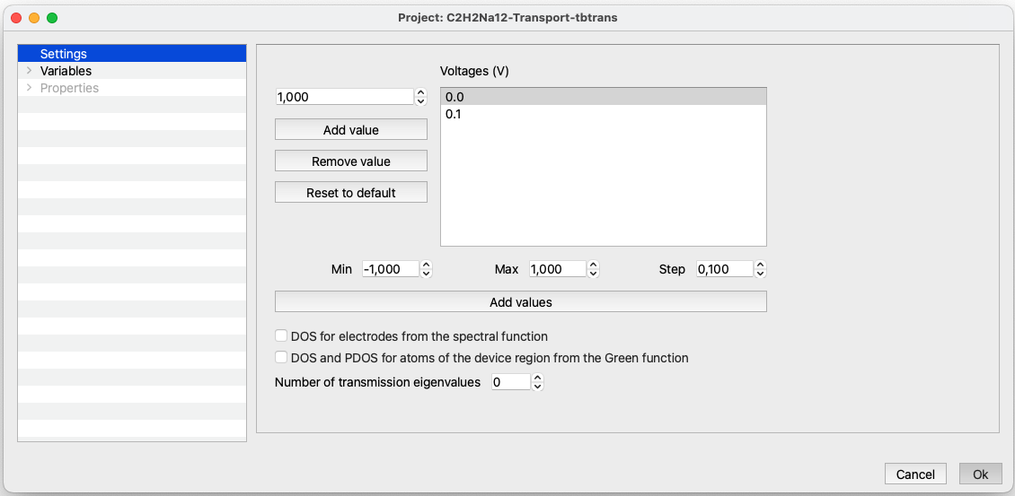
Click on the Parameters icon to open the widget to set up the input
parameters related to transport postprocessing project.
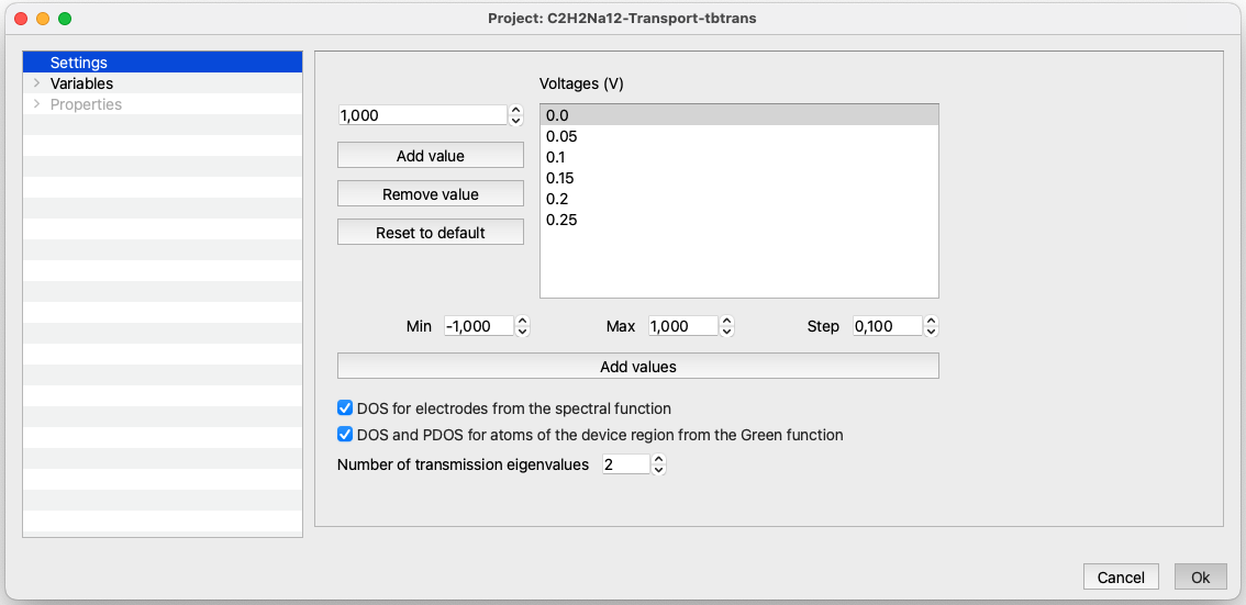
Fig. 25 Parameter widget for Transport post-processing project type.#
We describe below the parameters included in the Setting tab.
The list of voltages used in the completed electronic transport calculation
is shown by default. You can introduce extra values of voltages (values used
during the interpolation) by using the following buttons:
Add value: To add a value to the list of voltages. Each value will be
applied to the system along the transport direction.
Remove value: To remove the selected voltage value from the list on the
right.
Reset to default: To reset to default voltage values.
You can also create automatically a list of voltage values. Use the
parameters at the bottom of the widget to introduce the minimum (Min)
and maximum (Max) voltage and the interval between values (Step).
Then, press the Add values button.
In this window, you can specify whether you want to compute the DOS for
electrodes from the spectral function and the DOS and PDOS for atoms of
the device region from the Green function. Additionally, you can indicate
the maximal Number of transmission eigenvalues to compute.
Press the OK button to close the widget after the parameters are
properly set.
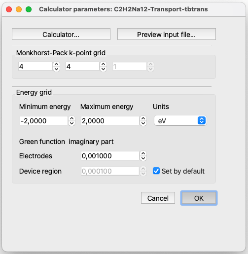
Notice that in the new project, the calculator is TBTRANS 4.1 (Tight-Binding
transport) code. TBTRANS is a code to calculate electronic transport and
other physical quantities using the Green function formalism. Click on the
TBTRANS 4.1 icon to open the calculator parameter widget.
You can tune the following variables:
Monkhorst-Pack k-point grid: To specify the number of k-points
distributed homogeneously in the Brillouin zone.
Energy grid: To define the energy range (minimum and maximum energy)
for the integration. In units of eV, meV, Rydberg or Hartree.
Green function imaginary part: Control the imaginary energy of the
surface Green function in the electrodes and in the device region.
Press the OK button to close the widget after the parameters are
properly set.
Click on the Run icon to open the Run widget. Then click on the Run
button to submit calculations required to post process the output of the
completed transport calculation.
Transport postprocessing workflow: Analysis
Once the calculation is completed, click on the Exit & Analyse… button
to open the transport analysis widget.
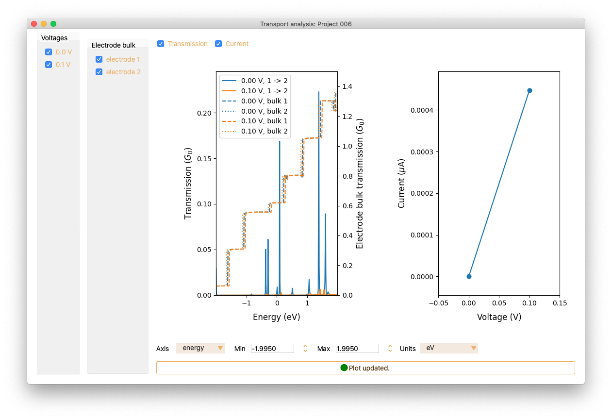
The transport analysis widget shows the Transmission (left figure) and the
Current (right figure) through the device. You can enable/disable each of
the plots.
You can also visualise the contribution to the Transmission and Current of
each electrode by clicking on the electrode 1 and/or electrode 2 radio
buttons.
At the bottom of the widget, you can indicate the minimum and maximum energy
(voltage) and desired units.
In the bottom area of the widget, the minimum and maximum energy/voltage can
be set in different units.